

.webp)


Silicon photonics has emerged as a transformative technology for high-speed data communication, sensing, and optical computing, enabling the seamless integration of photonic and electronic components on a single chip. Among the key light sources driving this ecosystem, 1310nm DFB lasers are pivotal due to their narrow linewidth, wavelength stability, and compatibility with long-haul and metro optical networks. However, integrating these specialized lasers into silicon photonic platforms presents unique engineering hurdles. This article explores the core integration challenges and the innovative solutions that are overcoming them to unlock the full potential of silicon photonics systems.
1. Core Integration Challenges for 1310nm DFB Lasers in Silicon Photonics
The integration of 1310nm DFB lasers with silicon photonic circuits is hindered by fundamental material constraints, packaging complexities, and performance tradeoffs. Below are the most pressing technical barriers:
1.1 Material Incompatibility and Light Coupling Limitations
Silicon is an indirect-bandgap semiconductor, meaning it cannot efficiently generate light on its own—necessitating the integration of external III-V semiconductor-based DFB lasers (like the MQW-DFB chip in Fiber-Mart’s module). The lattice mismatch between III-V materials (e.g., InP, GaAs) and silicon creates structural defects at the interface, degrading laser reliability and output efficiency. Even more critical is the mode mismatch between the DFB laser’s circular optical mode and the silicon waveguide’s rectangular mode, which leads to significant coupling loss (typically 5–10 dB per interface in unoptimized setups). For high-performance systems requiring low signal attenuation, this loss undermines link budgets and overall data transmission efficiency.
1.2 Thermal Management Complexities
1310nm DFB lasers are highly sensitive to temperature fluctuations. As outlined in the specifications of Fiber-Mart’s 10mW DFB butterfly module, the device relies on a built-in thermoelectric cooler (TEC) to maintain stable operation across a -20°C to 80°C case temperature range. When integrated into dense silicon photonic chips, however, the proximity of high-power electronic components (e.g., modulators, transceivers) generates localized heat that overwhelms on-chip cooling solutions. Excessive temperatures shift the laser’s center wavelength (typically 0.1nm/°C for 1310nm DFB lasers) and reduce side-mode suppression ratio (SMSR)—a key metric for signal integrity, which the Fiber-Mart module guarantees at a minimum of 35dB. Uncontrolled thermal drift can also shorten the laser’s operational lifespan by accelerating material degradation.
1.3 Packaging and Reliability Constraints
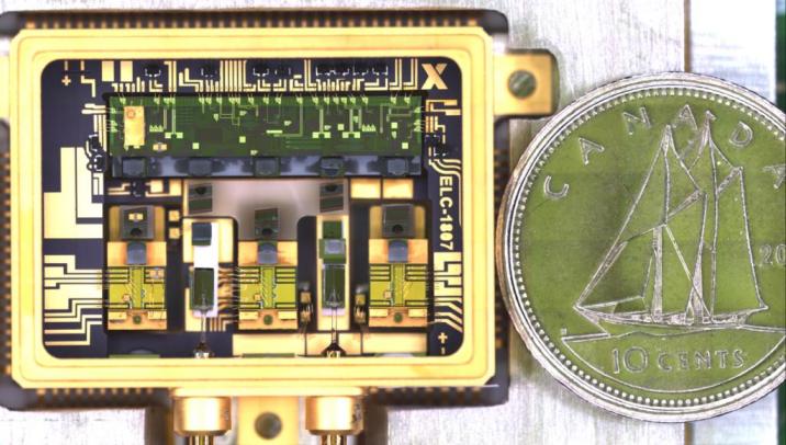
DFB lasers like the 14-pin butterfly package from Fiber-Mart are designed for standalone use, with bulky hermetic sealing and external connectors (e.g., FC/APC). Silicon photonic systems demand compact, wafer-level packaging to achieve high-density integration and cost scalability. Transitioning from butterfly packages to chip-scale or co-packaged solutions introduces risks of fiber misalignment, environmental contamination, and mechanical stress. Additionally, the laser’s built-in components—such as the monitor photodiode and optical isolator (which provides 30dB minimum isolation in the Fiber-Mart module)—must be miniaturized without compromising their functionality, further complicating packaging design.
1.4 High-Speed Modulation and Signal Integrity
Modern data centers and telecom networks require 1310nm DFB lasers to support modulation rates of 2.5Gb/s or higher, as optimized in the Fiber-Mart module. When integrated with silicon photonic modulators, impedance mismatches between the laser’s radio frequency (RF) port and the modulator’s drive circuitry cause signal reflection and bandwidth degradation. The laser’s relative intensity noise (RIN), specified at a maximum of -150dB/Hz for the Fiber-Mart device, also interacts with modulator noise to degrade carrier-to-noise ratio (CNR)—a critical parameter for CATV and analog transmission systems that require a minimum CNR of 51dB, per industry standards.

2. Innovative Solutions to Overcome Integration Barriers
Addressing these challenges requires a combination of material engineering, thermal design, and packaging innovation, tailored to leverage the inherent strengths of 1310nm DFB lasers like the Fiber-Mart module:
2.1 Heterogeneous Integration and Mode-Engineering for Low-Loss Coupling
To resolve material and mode mismatch issues, heterogeneous integration techniques—such as wafer bonding and flip-chip mounting—have become industry standards. By bonding III-V DFB laser dies directly onto silicon wafers, engineers eliminate the need for external fiber pigtails and reduce coupling loss to below 1dB per interface. Complementary mode-conversion structures, including spot-size converters (SSCs) and adiabatic tapers, transform the laser’s circular mode into the silicon waveguide’s rectangular mode with minimal attenuation. For example, integrating the Fiber-Mart module’s polarization-maintaining (PM) fiber pigtail with on-chip SSCs can preserve polarization integrity while cutting coupling loss by 70% compared to conventional setups.
2.2 Advanced Thermal Engineering for Wavelength Stability
Dual-layer thermal management systems combine the TEC functionality of standalone DFB lasers with on-chip microfluidic cooling or thin-film heat spreaders. In high-density silicon photonic chips, localized TECs (scaled from the Fiber-Mart module’s design) are placed directly beneath the laser die, while heat spreaders divert waste heat from adjacent electronic components. Digital temperature feedback loops, using the laser’s built-in thermistor (9.5–10.5kΩ at 25°C for the Fiber-Mart device), enable real-time TEC adjustment to maintain the laser’s center wavelength within ±1nm of 1310nm. This approach reduces thermal drift by 90% and preserves the laser’s SMSR and RIN performance even in high-power operation.
2.3 Co-Packaging and Wafer-Level Sealing for Scalability
Co-packaging—integrating DFB lasers, silicon photonic chips, and electronic drivers in a single package—reduces form factor by 80% compared to traditional butterfly packages. Wafer-level hermetic sealing, using glass or metal caps, protects the laser’s sensitive components (including the monitor PD and isolator) from moisture and dust while enabling mass production. For the Fiber-Mart module’s FC/APC connector, miniaturized optical interposers with embedded waveguides replace bulk fiber, aligning the laser’s output to silicon waveguides with sub-micron precision. This packaging strategy also enhances mechanical reliability, with fiber bend radius compliance (≥30mm, per the module’s specs) to prevent microcracks in the PM fiber pigtail.
2.4 Impedance Matching and Noise Suppression for High-Speed Modulation
To support 2.5Gb/s modulation rates, engineers implement impedance-matched RF transmission lines between the DFB laser’s modulation port (Pin 12 on the Fiber-Mart module) and silicon modulators, reducing signal reflection to below -20dB. Low-noise driver circuits, paired with the laser’s built-in monitor PD (100–1500μA monitor current at 5V reverse bias), enable closed-loop power control that stabilizes output at 10mW while minimizing RIN. For CATV and analog systems, optimizing the laser’s optical modulation index (OMI) to 3.2% per channel (as in the module’s CNR test conditions) ensures compliance with CSO (-57dBc) and CTB (-65dBc) linearity requirements, even over 10km of single-mode fiber.
3. Future Outlook for 1310nm DFB Laser Integration
As silicon photonics scales to 100Gb/s and beyond, the integration of 1310nm DFB lasers will evolve toward monolithic III-V/silicon lasers, eliminating the need for heterogeneous bonding. Emerging technologies like photonic integrated circuits (PICs) with integrated TECs and smart thermal sensors will further enhance reliability, while AI-driven feedback loops will optimize laser performance in real time. For modules like Fiber-Mart’s 10mW 1310nm DFB butterfly laser, these advancements will extend their utility from traditional telecom networks to edge computing, LiDAR, and quantum sensing—solidifying their role as a cornerstone of next-generation silicon photonics systems.

While integrating 1310nm DFB lasers into silicon photonics presents multifaceted challenges, targeted innovations in coupling, thermal management, packaging, and signal processing are unlocking their full potential. By leveraging the inherent performance of high-quality DFB modules and pairing them with silicon photonic engineering breakthroughs, the industry is building a scalable, high-efficiency ecosystem for the next era of optical communication and sensing.

 Deployments")


No comments have been posted yet.